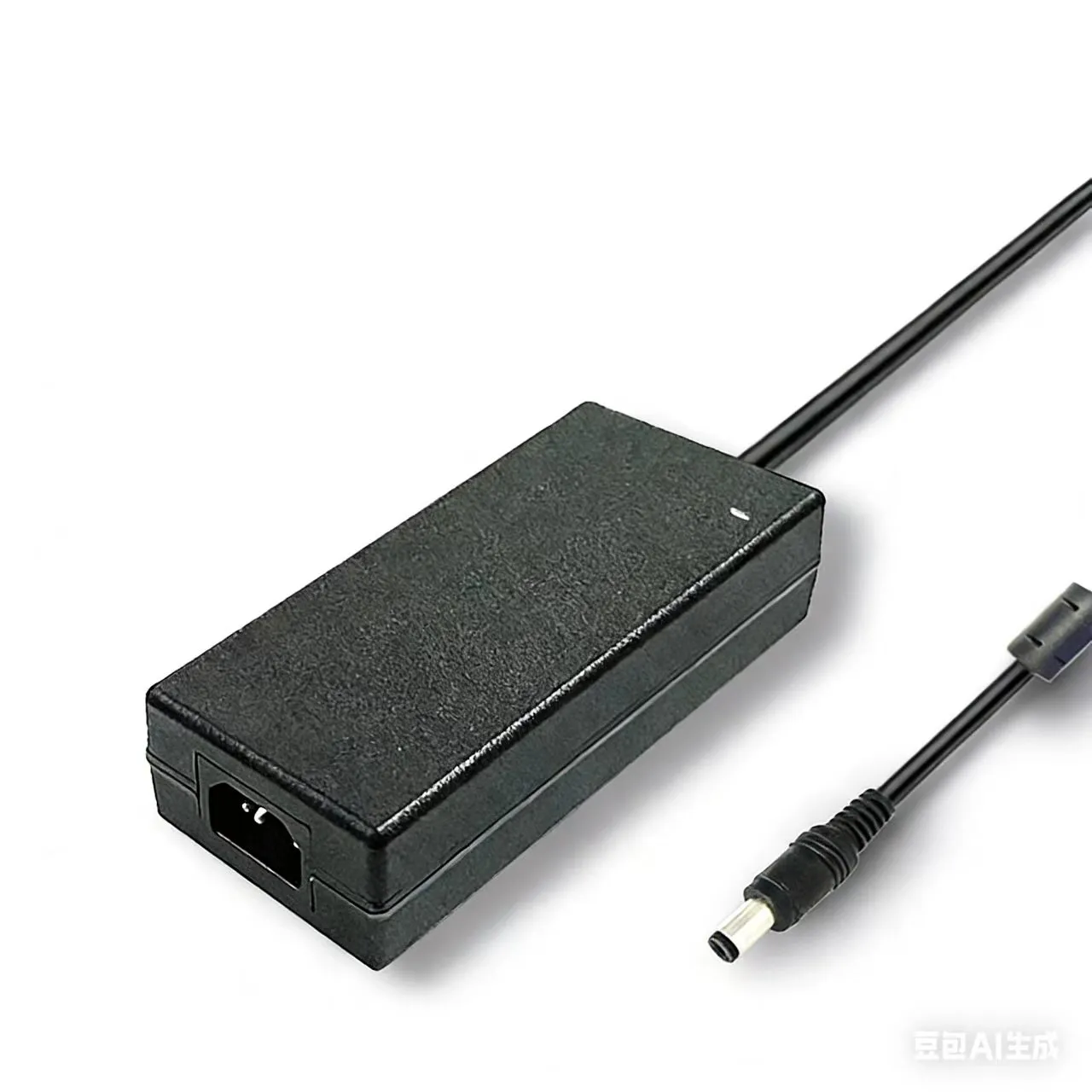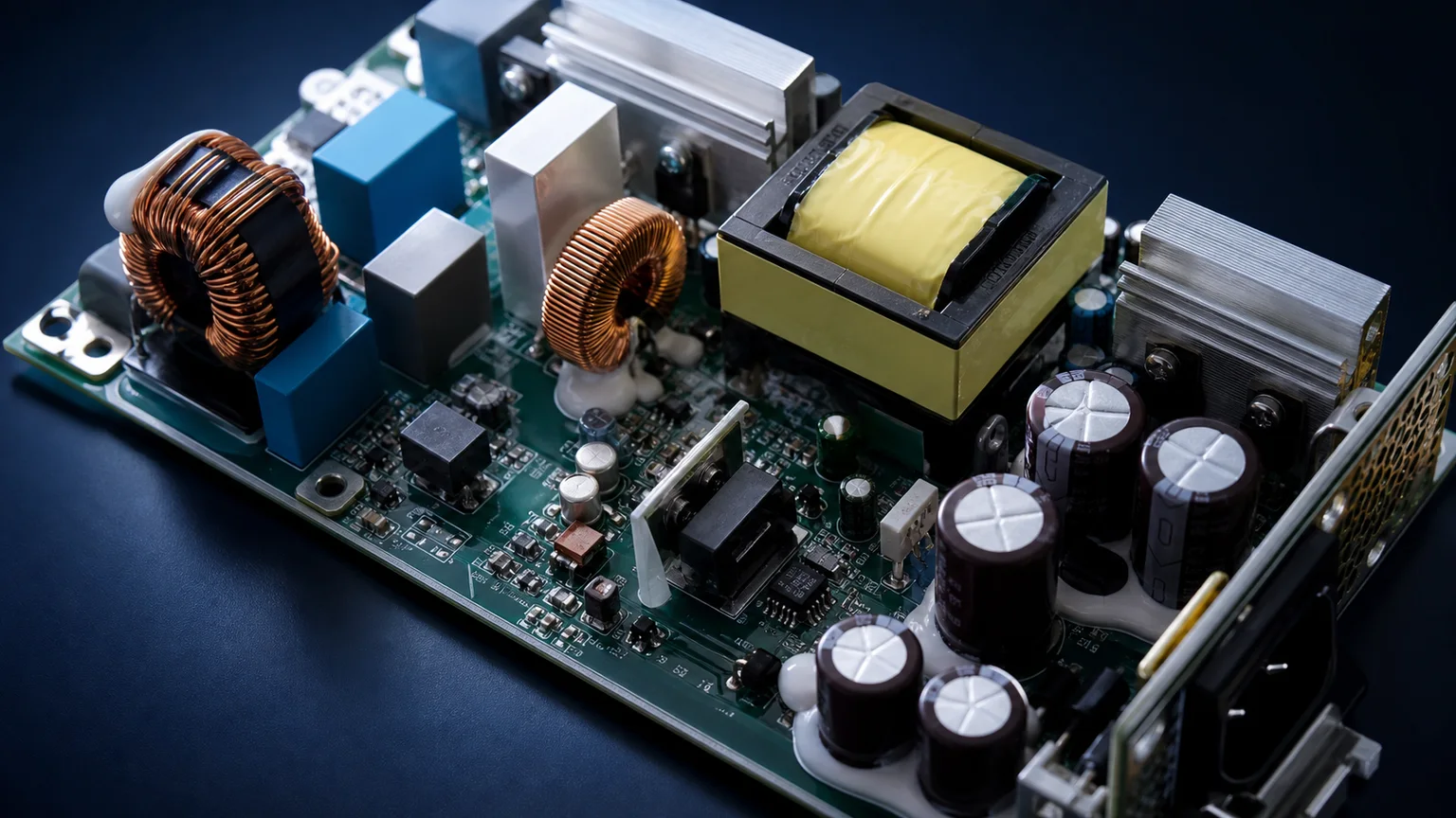

A 240W desktop adapter came back from the lab at 89% efficiency with its output rectifier diodes too hot to touch — a 12°C rise above the rest of the board. The fix changed no transformer, no PFC stage, no controller. The team replaced the secondary Schottky diodes with synchronous rectification (SR) MOSFETs and an SR controller, and the same unit measured 94% efficiency with the rectifier temperature down 12°C. That single swap is the difference between a 80 PLUS Bronze-class number and a Platinum-equivalent one, and it lives entirely in how the supply turns AC into DC at the output rectifier.
This guide covers power supply synchronous rectification vs Schottky diode MOSFET efficiency selection — the output-side decision one stage downstream of the LLC resonant vs hard-switched topology choice and one device generation alongside the GaN vs silicon switch-material choice. Topology decides how you convert; rectification decides how cleanly you collect the result.
Why 80 PLUS Platinum and Titanium Demand Synchronous Rectification
Efficiency tiers are won and lost in fractions of a percent, and the output rectifier is where the largest single chunk of conduction loss hides. In a 5V/20A output, every diode in the path drops its forward voltage across the full output current — raw watts converted to heat, on every cycle. At Platinum and Titanium tiers (≥92% and ≥94% across the load range), that rectifier loss alone can be the gap between passing and failing. SR is effectively mandatory here, because no Schottky diode has a low enough forward drop to leave headroom for the rest of the budget.
Three Generations of Rectification: PN Diode, Schottky, Synchronous
Output rectification has evolved through three stages, each cutting the voltage drop — and therefore the loss — by roughly half:
| Generation | Drop across device | Loss at 20A | Typical application | Cost index |
|---|---|---|---|---|
| Standard PN diode | Vf ≈ 0.7 V | ~14 W | Legacy, high-voltage, low-current rails | 1× |
| Schottky barrier diode (SBD) | Vf ≈ 0.3–0.5 V | ~6–10 W | 12V/24V/48V outputs, moderate current | 1.5× |
| Synchronous rectification (SR) | Vds = I × Rds(on) ≈ 20–60 mV | ~0.4–1.2 W | Low-voltage high-current, Platinum/Titanium | 3–4× |
A PN diode wastes the most, a Schottky roughly halves it, and an SR MOSFET — dropping only the product of current and on-resistance — cuts loss by another order of magnitude. Cost and complexity climb in step, which is why the choice is never automatic.
Schottky Barrier Diode (SBD) in Detail
A Schottky diode replaces the silicon PN junction with a metal-semiconductor junction. That structure gives it two defining traits: a low forward voltage of 0.3–0.5V (versus ~0.7V for PN), and an almost negligible reverse-recovery charge (Qrr), because conduction is by majority carriers — there is no stored minority charge to sweep out when the device turns off. That makes SBDs fast and clean switchers, ideal for high-frequency rectification.
Their weaknesses are equally structural. Schottky diodes have higher reverse leakage than PN diodes, rising steeply with temperature and reverse voltage — a thermal-runaway risk near the rated blocking voltage. They are most at home on higher-voltage, lower-current outputs (12V, 24V, 48V and above), where the fixed 0.3–0.5V drop is a small fraction of the output. On a 5V rail, that same 0.4V is 8% of the output — exactly where SR takes over.
Synchronous Rectification (SR) in Detail
Synchronous rectification replaces the diode with an N-channel MOSFET connected to conduct in the direction current naturally flows, turned on actively when it should conduct. Because a MOSFET in its on-state behaves as a small resistor, the voltage across it is Vds = Iout × Rds(on) — for a 3mΩ device at 20A, just 60mV, against a Schottky's 400mV. Paralleling devices or picking a lower-Rds(on) part keeps cutting it.
Every SR MOSFET also carries an intrinsic body diode between source and drain. This matters: when the gate turns off — and during dead time — the body diode carries the output current just like an ordinary (poor, ~0.8V) diode. It is a safety net, not the working path; the art of SR is keeping current in the low-resistance channel and out of the body diode for as much of each cycle as possible. That makes gate-drive timing the core engineering problem, not the MOSFET itself.
SR Drive Schemes: Self-Driven, Control-Driven, and SR Controller IC
There are three ways to generate the SR gate signal, and they trade reliability against simplicity:
| Drive scheme | How the gate is driven | Reliability | Complexity | Cost | Typical IC |
|---|---|---|---|---|---|
| Self-driven | Gate taken from a transformer secondary winding | Low (poor at light load / burst) | Lowest | Lowest | None (winding + RC) |
| Control-driven | PWM controller synchronizes SR with primary | Medium | Medium | Medium | Primary controller w/ SR output |
| SR controller IC | IC senses MOSFET Vds and turns on adaptively | High | Higher | Higher | UCC24612, NCP4308 (industry examples) |
Self-driven SR is cheapest — the gate comes straight off an auxiliary winding — but it tracks the transformer voltage, not the actual current, so it misbehaves under burst mode and light load. Control-driven SR ties the SR timing to the primary PWM, improving coordination at a moderate cost. Dedicated SR controller ICs (UCC24612, NCP4308 and similar parts are common industry references, named here only as generic examples) sense the MOSFET's own Vds to detect conduction and switch adaptively — the most robust approach, and the standard for high-efficiency designs. Sanyi's high-power platforms use the controller-IC approach for exactly this reliability margin.
Dead Time and Shoot-Through Prevention
In any SR design where two devices alternate (the two halves of a center-tapped or full-bridge secondary), both must never conduct at once. If the incoming switch turns on before the outgoing one is fully off, the two create a momentary short across the winding — shoot-through — and the resulting current spike can destroy the MOSFETs. The defense is dead time: a deliberate gap, typically 50–200ns, where both gates are low.
Dead time is a balance, not a maximum. Too short risks shoot-through. Too long forces the body diode to carry current during the gap — at ~0.8V instead of 60mV — adding loss and partly squandering the efficiency SR was meant to deliver. Optimizing dead time to the specific MOSFET and frequency is one of the highest-leverage tuning steps in an SR design.
Rds(on) and Current: Practical Engineering Match
Choosing Rds(on) balances conduction loss, switching loss (lower-Rds(on) parts have higher gate charge), voltage rating, and cost. Two rules anchor it: the device must block at least 1.5× the peak reverse voltage it sees, and you must account for Rds(on) rising roughly 30% at 100°C versus its 25°C datasheet value. A part chosen at its cold spec runs hotter and lossier than expected in the field.
| Output | 5A | 10A | 20A |
|---|---|---|---|
| 5V | < 12 mΩ | < 8 mΩ | < 5 mΩ |
| 12V | < 20 mΩ | < 10 mΩ | < 6 mΩ |
| 24V | < 30 mΩ | < 18 mΩ | < 10 mΩ |
These ranges target a Vds drop low enough to keep rectifier loss in the sub-1% range of output power; tighten them where the thermal budget is tight, and confirm the voltage rating against the secondary's peak reverse swing plus ringing margin.
SR Across Topologies: LLC, Flyback, Forward, Half/Full-Bridge
Where SR sits depends on the converter:
- LLC resonant — SR replaces the secondary diodes in the center-tapped or push-pull rectifier. LLC is especially SR-friendly because its quasi-sinusoidal secondary current crosses zero cleanly, giving a well-defined turn-off point (near-ZCS).
- Flyback — SR replaces the single output Schottky. The discontinuous, sharply-edged current makes timing harder, so a good SR controller IC matters more here.
- Forward — Needs two SR MOSFETs: one for forward conduction and one for the freewheeling path, both synchronized.
- Half / full-bridge — A full-bridge secondary rectifier becomes four synchronized SR MOSFETs, the most complex case but also the highest-current, where SR pays back most.
SBD vs SR: Side-by-Side Selection
When the output point is genuinely borderline, weigh the two technologies across every axis at once rather than on efficiency alone:
| Criterion | Schottky diode (SBD) | Synchronous rectification (SR) |
|---|---|---|
| Voltage drop / loss | Vf 0.3–0.5V, fixed | Vds = I×Rds(on), tens of mV |
| Efficiency at high current | Lower | Higher (often +3–5 points) |
| Complexity | Minimal (passive) | Higher (gate drive + timing) |
| EMI | Recovery spikes possible | Cleaner if timed well |
| Cost | Lower | Higher (MOSFET + controller) |
| Thermal design | Heatsink often needed | Lower rise, easier |
| Best fit | High-V, low-current rails | Low-V, high-current outputs |
| Reliability concern | Reverse leakage at temperature | Shoot-through if mistimed |
The decision rule: pick SBD where output voltage is high and current modest; pick SR wherever conduction loss dominates the efficiency budget — every Platinum/Titanium-class low-voltage, high-current rail.
SR vs GaN/SiC Rectification
SR and wide-bandgap devices are complementary, not competing. At very high switching frequencies (into the MHz range), GaN SR MOSFETs are increasingly common because their tiny gate charge and near-zero reverse recovery suit fast soft-switched stages. SiC dominates high-voltage rectification (1200V bus rails) where silicon can't block enough. For mainstream 5V–48V AC-DC outputs, silicon SR MOSFETs remain the workhorse — GaN and SiC extend the envelope rather than replace it, the same device-material spectrum from our GaN vs silicon guide applied to the rectifier.
Five Common SR Design Pitfalls
- Self-driven SR misfiring in burst mode — At light load the transformer voltage driving a self-driven gate becomes erratic, falsely turning the SR on and causing reverse current. Use a controller IC.
- SR controller Vds threshold set too tight — Too aggressive a conduction-detect threshold misses low-load conduction and forces current into the body diode. Tune it to the load range.
- Parasitic-inductance ringing at turn-off — Stray loop inductance rings against the MOSFET capacitance when SR turns off; an RC snubber and tight layout tame it.
- Kelvin-source mis-wiring — Routing the gate-driver return to the power-source pad instead of a Kelvin-source connection injects switching noise into the gate loop, causing false triggering. Always use a Kelvin-source.
- Body-diode reverse recovery under heavy load — If dead time forces the body diode to conduct, its reverse recovery on the next turn-on produces an EMI spike. Minimize dead-time body-diode conduction and snub where needed.
The Sanyi Synchronous Rectification Product Ecosystem
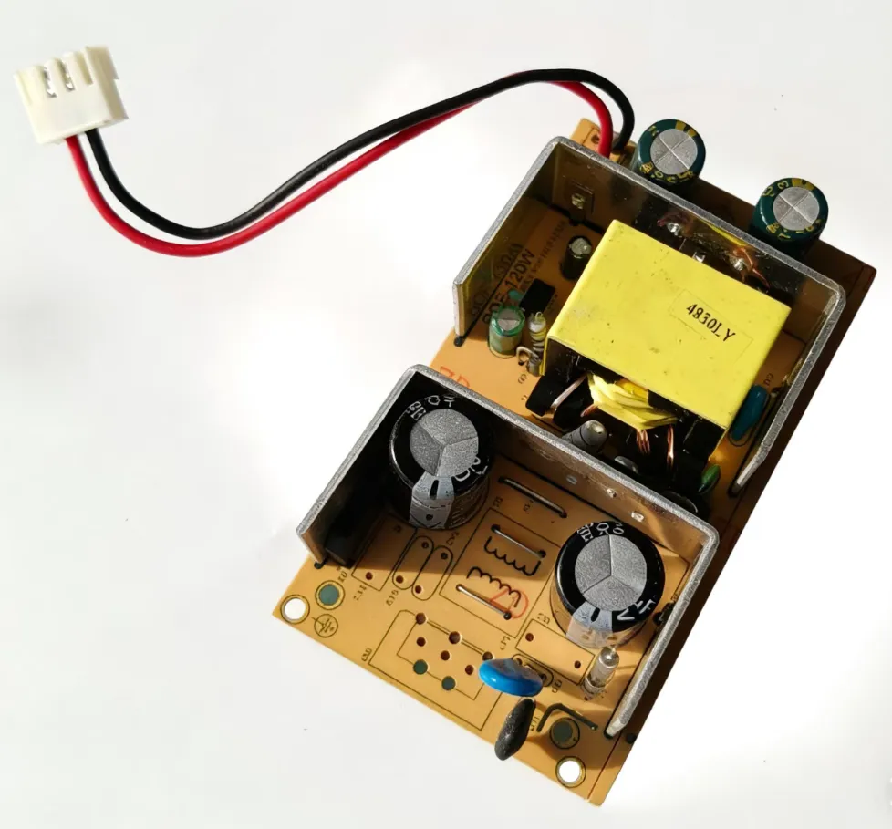
Sanyi's high-power adapter and charger lines are built around synchronous rectification with dedicated SR controller ICs, targeting 92–96% efficiency (80 PLUS Platinum-equivalent) across the load range. The HP-series high-power desktop adapters (up to 240W) and the APN-series desktop adapters use SR on the secondary to keep rectifier loss and temperature rise low at high output current. For multi-port and high-current charging, the SY-C260W smart charger and the higher-power SY-C500W charger pair an efficient back end with output-side SR. The same output-ripple care SR enables is covered in our output ripple & noise (PARD) measurement guide.
Frequently Asked Questions
Is synchronous rectification always better than a Schottky diode? No. SR wins decisively on low-voltage, high-current outputs (5V/12V at tens of amps), where the diode's fixed forward drop is a large fraction of the output. On high-voltage, low-current rails, a Schottky's 0.3–0.5V drop is a small percentage of output, and its simplicity and lower cost often win. Match the technology to the output point.
Why is self-driven SR unreliable at light load? A self-driven gate follows the transformer voltage rather than the actual current. Under burst mode or very light load the winding voltage becomes intermittent and ill-timed, falsely turning the SR on during reverse conduction. A Vds-sensing SR controller IC reads the MOSFET's real conduction state and stays reliable across the load range.
How much dead time should I use? Typically 50–200ns, tuned to the specific MOSFET and switching frequency. Too short risks shoot-through; too long forces the body diode to carry current at ~0.8V, adding loss. Optimize it experimentally rather than copying a fixed number.
Is SR worth it on a 12V output? Often yes at higher currents. At 12V/10A a Schottky drops ~0.4V × 10A = 4W, while a 6mΩ SR drops ~0.06V × 10A = 0.6W — a meaningful gain. At a few amps the saving shrinks and a Schottky may be the simpler, cheaper choice. Run the numbers for your current.
How do I choose an SR controller IC? Match the controller to the topology (LLC, flyback, forward), the switching frequency, the Vds-detection threshold range, and the gate-drive strength your MOSFET needs. Industry-standard parts such as UCC24612 and NCP4308 are common reference examples; prioritize adaptive Vds sensing and a threshold suited to your load range.
.webp)