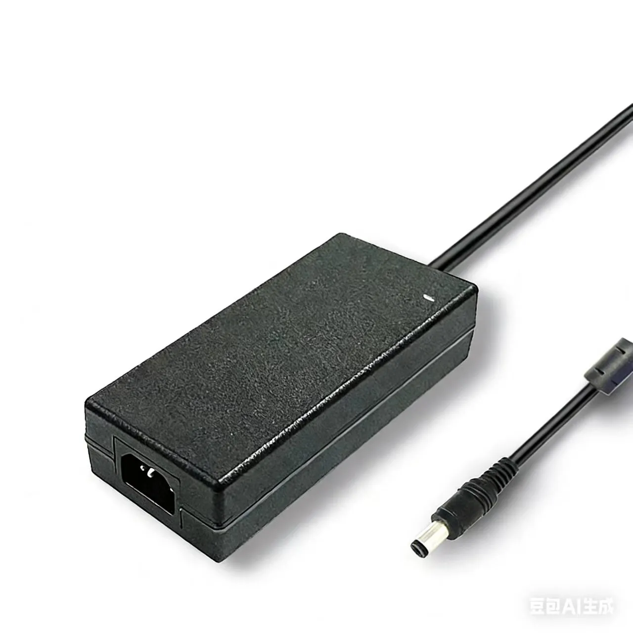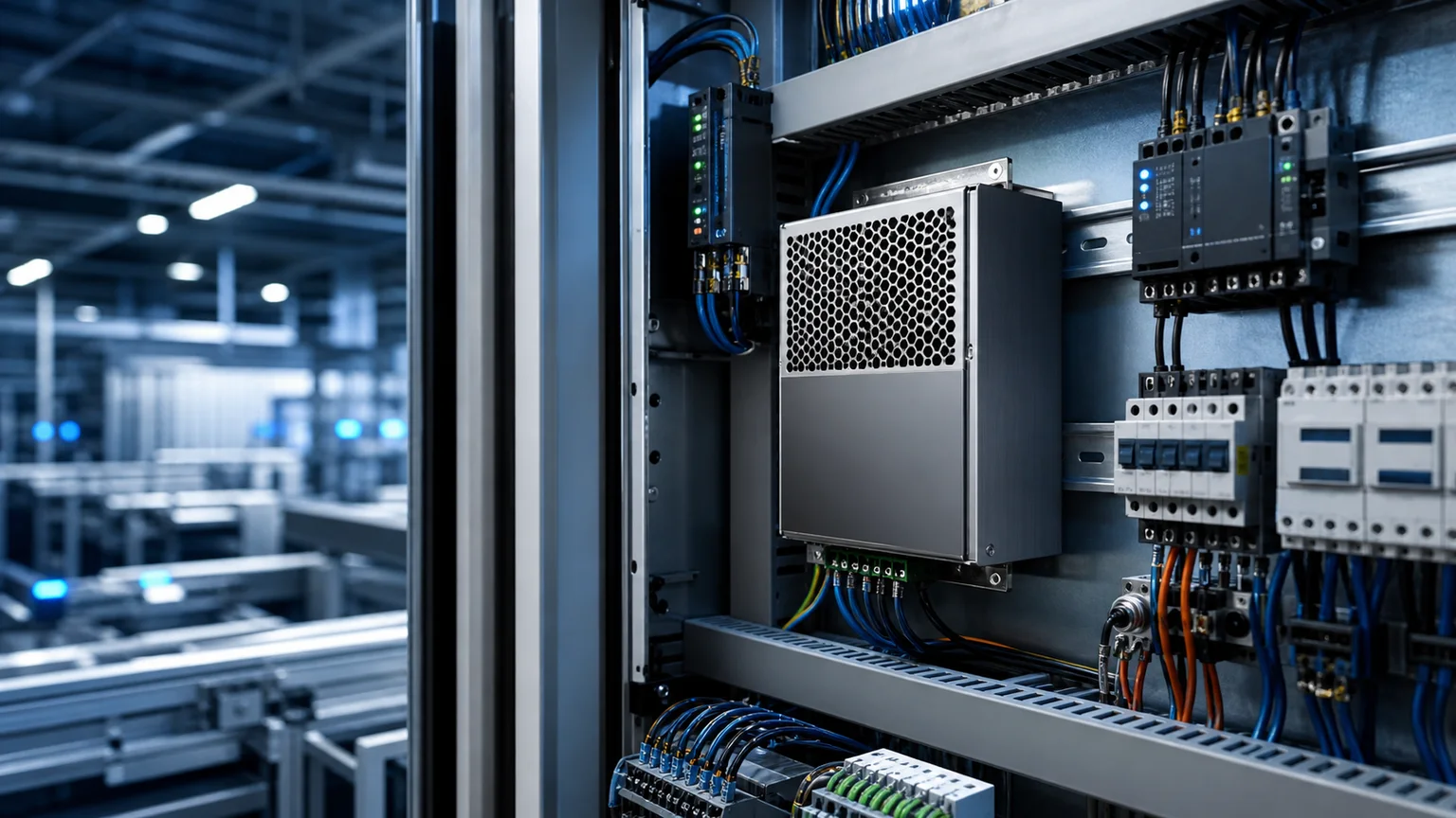

An embedded controller resets at random. Not in the lab, only in the field — and only when a nearby motor or relay energizes. The team checks the power supply: steady-state ripple is ≤ 50 mV, dead in spec, line and load regulation both immaculate. Then someone puts a scope on the 5 V rail with the right trigger and catches it: the moment the load steps, the output dives to 4.3 V in 8 µs before clawing back. That 700 mV undershoot punched straight through the MCU's 4.5 V brownout threshold and tripped the watchdog. The datasheet was never wrong. It simply described a steady output, and the failure lives in the transient.
This guide explains how load transient response is actually defined and measured on switching power supplies and adapters: the five performance metrics that matter, how a load step is standardized, where the undershoot voltage physically comes from, how to choose output capacitors and a control loop to contain it, and the measurement pitfalls that turn a good supply into a false reject or a good design into a field failure.
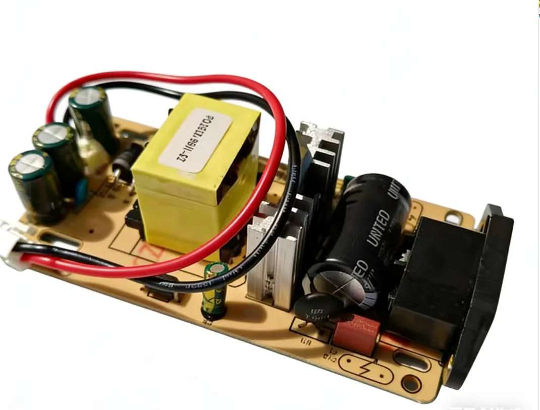
The Five Dynamic Performance Metrics
A single "transient response" number means nothing without saying which number. A load step produces a full waveform, and five metrics describe it:
- Undershoot ΔV_d — the maximum dip below nominal when the load increases (the dangerous one for brownout).
- Overshoot ΔV_o — the maximum rise above nominal when the load decreases (the dangerous one for downstream OVP and capacitor stress).
- Settling time t_set — time from the load edge until the output re-enters a defined band (often ±1% of V_nom).
- Recovery time t_rec — time to recover to the regulation band, sometimes quoted separately from full settling when ringing decays slowly.
- Dynamic regulation % — the worst-case deviation expressed as a percentage of V_nom, the headline figure on a spec line.
Crucially, these are not static line/load regulation. Static regulation is the DC offset between two steady operating points measured with a multimeter; dynamic response is the AC excursion during the change, measured with a scope. A supply can hold 0.5% static load regulation and still undershoot 8% on a fast step.
| Metric | Symbol | Definition | Typical industrial target |
|---|---|---|---|
| Undershoot | ΔV_d | Max dip on load increase | ≤ 3–5% V_nom |
| Overshoot | ΔV_o | Max rise on load decrease | ≤ 3–5% V_nom |
| Settling time | t_set | Return to ±1% band | ≤ 100–500 µs |
| Recovery time | t_rec | Return to regulation band | ≤ 200 µs |
| Dynamic regulation | — | Worst deviation as % V_nom | ≤ 5% V_nom |
Standardizing the Load Step: Amplitude, di/dt and Repetition
The transient number is only meaningful with its stimulus pinned down, because a slow step hides what a fast one exposes:
- Step amplitude — common standardized steps are 50%→100%, 10%→90%, and the brutal 0%→100%. A bigger ΔI means a bigger ΔV, so always read the amplitude with the number.
- Slew rate di/dt — how fast the current changes. The widely used electronic-load fixture value is 2.5 A/µs, with 1 A/µs and a slow 0.1 A/µs as softer references. A higher di/dt forces a deeper undershoot because the control loop has even less time to react.
- Single-shot vs repetitive — a one-time single-shot step characterizes the worst case; a repetitive step (e.g., 100 Hz or 1 kHz, 50/50 duty) reveals thermal and recovery behavior under sustained cycling.
Quoting "ΔV ≤ 3%" without the amplitude, di/dt, and repetition is unverifiable — the same supply can read 3% at 0.1 A/µs and 9% at 2.5 A/µs.
Where the Undershoot Comes From: ESR Drop + Bulk Discharge
The dip during a load step is the sum of two distinct physical mechanisms, and confusing them leads to the wrong fix:
- ESR instantaneous drop — the moment current jumps by ΔI, the output capacitor's equivalent series resistance produces a step ΔV = ΔI × ESR. This is essentially instantaneous (nanoseconds), depends only on ESR, and is independent of capacitance. Adding more of a high-ESR capacitor does nothing here.
- Bulk discharge during loop delay — for the time Δt_loop it takes the control loop to react and command more current, the output capacitor alone supplies the extra load, drooping by ΔV = ΔI × Δt_loop / C. This term is set by capacitance and by loop speed.
Total undershoot ≈ ESR step + bulk-discharge droop. The practical consequence: if your dip is ESR-dominated, you need lower-ESR capacitors; if it is droop-dominated, you need more capacitance or a faster loop. Throwing capacitance at an ESR problem wastes board space and money.
Output Capacitor Selection Matrix
No single dielectric wins on every axis. The transient designer trades ESR against capacitance density, lifetime, and DC-bias stability:
| Type | ESR (typ.) | Capacitance density | DC-bias loss | Lifetime / notes |
|---|---|---|---|---|
| Aluminum electrolytic | ~100 mΩ | High | None | Large value, high ESR, wear-out (ESR rises with age) |
| OS-CON / polymer | 5–30 mΩ | Medium | None | Balanced ESR + stable value, long life |
| MLCC array (X7R) | < 5 mΩ | Low–medium | Severe | Lowest ESR, but loses up to ~50% capacitance under DC bias |
| POSCAP (tantalum-polymer) | 10–40 mΩ | High | Mild | Compact, stable, mid ESR |
The classic transient combination is a polymer/OS-CON bulk element for charge storage paired with an MLCC array for the fast ESR/ESL floor — the ceramics kill the instantaneous ESR step while the polymer supplies bulk charge during the loop delay. Just remember to derate MLCC capacitance for DC bias: a "22 µF" X7R at its rated voltage may behave like 11 µF.
Loop Bandwidth and Crossover Frequency
How fast the loop reacts is set by the crossover frequency f_c — the frequency where open-loop gain falls to 0 dB. A useful rule of thumb is f_c ≈ 1/10 to 1/5 of the switching frequency f_sw: a 100 kHz converter typically lands at f_c = 10–20 kHz.
Higher f_c shrinks Δt_loop and therefore the undershoot — but pushing it too high erodes stability margin and lets switching-frequency noise into the loop. There is also a hierarchy to respect: a PFC pre-stage runs a deliberately slow loop (below ~5 kHz) to avoid distorting the input current, so the downstream DC/DC loop must be cleanly separated in bandwidth from it. Transient response is fundamentally a contest between how fast f_c reacts and how much charge the output capacitor can hold in the meantime.
Bode Plot and Stability Margins
You cannot chase a high f_c blindly — the loop has to stay stable. Two margins govern it, read off the Bode plot at and around crossover:
- Phase margin (PM) — how far the phase is from −360° (i.e., 180° away from instability) at f_c. Target PM ≥ 45°; 60° is the common industrial default for a well-damped, ring-free response.
- Gain margin (GM) — how much headroom in gain remains where the phase hits −360°. Target GM ≥ 10 dB.
The challenge is the output LC filter, a second-order section that contributes up to −180° of phase shift near its resonance — eating margin exactly where you need it. Worse, boost and flyback converters in CCM add a right-half-plane (RHP) zero that raises gain while subtracting phase, capping how high f_c can safely go. The compensation network exists to claw that phase back.
Compensation Networks: Type I vs II vs III
The compensator shapes loop gain and phase to hit f_c with adequate margin. Three families, escalating in capability:
- Type I — a pure integrator. Zero phase boost; only usable where the power stage already has benign phase (rare in switchers).
- Type II — one pole-zero pair, providing up to ~90° of phase boost. The standard choice for current-mode CCM converters, where peak current control already removes one of the LC poles.
- Type III — two pole-zero pairs, up to ~180° of phase boost. Required for voltage-mode CCM converters, where the full LC double pole must be compensated to recover phase at crossover.
Rule of thumb: if you are in voltage mode with a sharp LC double pole and you need a high f_c, you climb to Type III. If current-mode control has already split the poles, Type II is usually enough.
How Control Mode Shapes Transient Response
The control architecture itself sets the speed/stability/complexity trade before any compensation is tuned:
| Control mode | Transient speed | Stability | Complexity / notes |
|---|---|---|---|
| Voltage-mode | Slow | High (well-damped) | Needs Type III for LC double pole |
| Peak current-mode | Medium | Good | Needs slope compensation at D > 50% |
| Hysteretic (ripple) | Fastest | Loop-stable but ripple-dependent | Largest output ripple, frequency varies |
| Constant on-time (COT) | Fast | Good with adequate ESR | Pseudo-fixed frequency, simple, popular in POL |
The ranking for raw transient speed runs hysteretic > COT > peak current-mode > voltage-mode. But fast is not free: hysteretic control trades speed for higher ripple and a wandering switching frequency, which collides with the steady-state PARD budget — see our output ripple and noise PARD measurement guide for the quiescent counterpart of this dynamic test.
Test Setup: Electronic Load, Scope and Probing
A transient measurement is only as good as its fixture, and the same artifacts that corrupt ripple readings corrupt transient readings:
- Stimulus — an electronic load in CC step mode with a programmable slew-rate trigger is the standard tool; a homemade MOSFET + load resistor + signal generator works if the gate edge is fast enough. The load's slew rate must meet or exceed the spec di/dt or you will under-read.
- Scope setup — switch on the 20 MHz bandwidth limit, use AC coupling to lift the small ΔV off the DC pedestal, and use a 1× probe with a coaxial 50 Ω-terminated connection (or a short ground-spring tip) to avoid manufactured spikes.
- Measurement point — probe as close to the output terminals as physically possible. A mere 5 cm of PCB trace adds ~30 nH of parasitic inductance, which shows up as extra "undershoot" that the load near the terminals never actually sees.
This is the output-side dynamic dual of input-side dynamics — for AC dropout and bulk-cap sizing on the input, see our hold-up time and ride-through guide.
Six Transient Measurement and Design Pitfalls
- Probe ground-loop noise read as ΔV. A long ground lead rings with probe and scope capacitance, faking a deeper dip. Use a ground spring or coax termination and keep the loop area tiny.
- Electronic-load slew rate too slow. Testing at 0.1 A/µs when the field event is 2.5 A/µs badly under-estimates the real undershoot — the loop has 25× more time to react in the test than in reality.
- No AC coupling. Leaving DC coupling on lets the DC pedestal eat the vertical range, hiding the small-signal ΔV you are trying to measure. AC-couple and zoom in.
- MLCC DC-bias derating ignored. A "22 µF" ceramic at rated voltage may deliver ~11 µF, so the bulk-discharge droop is worse than the BOM suggests. Derate for DC bias before sizing.
- PCB output-trace ESL unmodeled. The parasitic inductance of output traces and connector pins adds to the apparent ESR step; model it and probe at the terminals, not downstream.
- Crossover near the LC resonance. Placing f_c too close to half the LC resonant frequency invites ringing and a long settling time — keep adequate separation and verify PM at the real crossover.
A related warning: an aging electrolytic's ESR rises over life, so a unit that meets ΔV new can drift out of spec years later — the same wear-out physics covered in our protection circuit design guide for the fault-side dual of normal dynamic behavior.
Sanyi Power Supply Ecosystem — Transient Response Designed In
Sanyi designs its USB-PD fast-charging, desktop, and industrial adapter lines to application-correct transient targets, not just a flattering steady-state number. Output stages pair OS-CON polymer bulk capacitors with MLCC arrays so the ESR step and the bulk-discharge droop are both contained, with the loop tuned for PM ≥ 45° stability while holding ΔV ≤ 3% V_nom and settling time ≤ 200 µs at a 50%→100% step with di/dt 2.5 A/µs. The HP high-power adapter series (up to 240W) carries the output network to hold dynamic targets at full load, and the APN desktop adapter series applies the same loop discipline across mid-power desktop and IT loads. For dense multi-port charging where fast GaN switching meets aggressive load steps, the SY-C260W multi-mode charger and the higher-output SY-C500W high-power charger balance switching speed against undershoot budget.
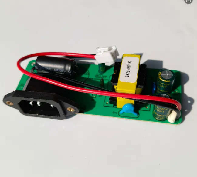
Because transient performance is a system trade — capacitor, loop, layout, and load all at once — our supplies are characterized to the step profile your application actually sees. Contact our power engineering team with your rail voltages, load-step amplitude, di/dt, and allowable ΔV, and we will recommend a platform with the matching output network and loop.
FAQ
What is the difference between dynamic regulation and static line/load regulation? Static line/load regulation is the steady-state DC offset between two stable operating points — you set the line or load, wait, and read a multimeter. Dynamic (transient) regulation is the momentary AC excursion during the change, measured on a scope. A supply can hold 0.5% static load regulation yet undershoot 8% on a fast 2.5 A/µs step, because the loop and output capacitor need time to respond. They are independent specs and both must be checked.
Can I just add more output capacitance to fix the undershoot? Only if the dip is droop-dominated. Total undershoot is an ESR step (ΔV = ΔI × ESR, independent of capacitance) plus a bulk-discharge droop (ΔV = ΔI × Δt_loop / C, set by capacitance and loop speed). If your dip is ESR-dominated, more high-ESR capacitance does almost nothing — you need lower-ESR parts or a faster loop. Diagnose which term dominates before changing the BOM.
How do I compensate for MLCC DC-bias capacitance loss? X7R/X5R ceramics lose effective capacitance under applied DC voltage — often up to ~50% at rated voltage. Always design with the derated value from the capacitor's bias curve, not the nameplate, and add headroom (e.g., choose a higher voltage rating or larger case size, or add parts) so the actual in-circuit capacitance still meets the bulk-discharge budget. Treating a 22 µF part as 22 µF in a transient calculation is a common cause of under-spec designs.
What phase margin is "stable enough" for transient response? Aim for PM ≥ 45° as the minimum and 60° as a well-damped industrial default, with gain margin ≥ 10 dB. Below ~45° the step response rings and settling time stretches; at 60° you get a clean, fast recovery with little overshoot. Verify the margin at the actual crossover frequency on the Bode plot, accounting for the LC double pole and any RHP zero in CCM boost/flyback stages.
My electronic load's slew rate is slower than the spec di/dt — what do I do? A slow load under-reports undershoot, so never trust a 0.1 A/µs result against a 2.5 A/µs requirement. Options: use a faster electronic load rated for the needed slew rate, build a MOSFET-based step circuit with a fast gate driver and a signal generator, or place the switched load close to the output terminals to minimize series inductance that limits di/dt. Always document the achieved slew rate alongside the ΔV number.
.webp)